BMFTR project "PicPhotMat ̶ Engineered materials for picophotonic analog computing"
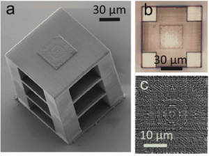
Scanning electron microscope (SEM) image (a) and optical microscope image (b) (top view) of a laser printed diffractive neural network. c) SEM image of a laser printed diffractive element.
Picture: E. Goi et al. (Nature Communications 13, 7531 (2022))Artificial intelligence (AI)-based methods, such as machine learning (ML) models, especially artificial neural networks (ANNs) have emerged into everyday life, with chatbots supporting customer service and generative AI writing emails. With the development of ML applications more performing than ever, the computational requirements for their execution are increasing exponentially, motivating efforts to develop new, specialized hardware for fast and efficient execution of neuromorphic models. High-end graphic processing units (GPUs) and other accelerators commonly used for running increasingly complex ANNs are hungry for power and bandwidth; they require substantial processing times and bulky form factors.
Matching algorithms to hardware hold the potential to lead toward faster and more energy-efficient information processing. Neuromorphic engineering aims to develop physical implementations of AI algorithms as hardware, to achieve systems with the ability of learning, deduce abstract concepts, and make decisions. Naturally, optics is a first-class candidate for building such analog processors for neuromorphic computing. By using photons instead of electrons, optical systems are excellent for handling large amounts of data quickly and can perform complex mathematical operations ̶ the fundamental building blocks of AI ̶ with much greater efficiency than traditional electronic processors.
The NanoPico Photonic Computing Group is a junior group funded by the BMFTR project "PicPhotMat ̶ Engineered materials for picophotonic analog computing". The group follows an innovative approach of utilizing the interaction between structured light and engineered materials for optical computation, with the goal of overcoming current constraints in integration- and computational density.
Main research areas
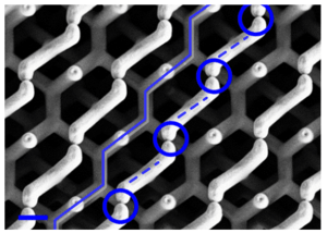
Scanning electron microscopy (SEM) images of the (–101) surface of a Weil point photonic crystal.
Picture: E. Goi et al. (Laser and photonic reviews 12, 1700271 (2017))· Development of fast, scalable optical probing systems for material characterization with sub-nanometer resolution.
· Design of 3D-printed, high-refractive-index functional metamaterials.
· Exploration of new optical information processing schemes using programmable optical elements.
· Study of light-matter interactions at the sub-nanometer and picometer scale.
Contact

Albert-Einstein-Straße 6
07745 Jena Google Maps site planExternal link

