The Nano & Quantum Optics group works in a rapidly developing research area that deals with the generation, propagation, manipulation, and detection of quantum light in structured systems with length scales down to the nanometer range. In close collaboration between scientists in theory, technology, and experimental characterization we try to understand the interplay between light and nanostructured systems and leverage this understanding for the development of new application concepts in different fields. Particular topics of the group, jointly headed by Thomas Pertsch and Frank Setzpfandt, cover e.g. the theoretical description of quantized and nonlinear light-matter interaction, the simulation of complex nanostructured systems, the development of advanced characterization methods for nanophotonics, and the development of applications using entangled light.
Highlights
Optical fibers covered with 2D material.
Illustration: C. Süß, Fraunhofer IOFScalable Functionalization of Optical Fibers Using Atomically Thin Semiconductors
Integrating atomically thin transition metal dichalcogenides into optical fibers yields novel opportunities in optical communication, remote sensing, and all‐fiber optoelectronics. However, the scalable and reproducible deposition of high‐quality monolayers on optical fibers was so far an unsolved challenge towards monolayer-functionalized integrated optical systems. Here we demonstrate chemical vapor deposition of monolayer MoS2 and WS2 crystals on the core of microstructured exposed‐core optical fibers. Their interaction with the fiber modes is reported, yielding the first true demonstration of monolayer-functionalized guided wave optics. Two distinct experiments demonstrate their application possibilities: first, the excitonic 2D material photoluminescence is simultaneously excited and collected with the fiber modes, opening a novel route to remote sensing. Then it is shown that third‐harmonic generation is modified by the highly localized nonlinear polarization of the monolayers, yielding a new avenue to tailor nonlinear optical processes in fibers. It is anticipated that the results may lead to significant advances in optical‐fiber‐based technologies.
Published in Advanced Materials DOI: 10.1002/adma.202003826 (2020)External link
Tunable visible light metasurface displays.
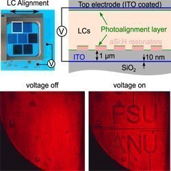
Image: IAP (University Jena)Tunable visible light metasurface displays
In recent years, tunable metasurfaces and metadevices have attracted extensive research efforts, aiming at pushing optical metasurfaces for practical applications. Infiltrating metasurfaces with nematic liquid crystals is an attractive approach due to its high compatibility with the existing industrial technologies and optical devices. Here, we demonstrated a LC-infiltrated metasurface with large transmittance modulation at red wavelengths for display applications. Different from conventional LC displays, the transmittance modulation takes place inside the subwavelength metasurface layer, rather than usually the bulk LC layer. Additionally, for the first time we use the technique of photoalignment to define and improve the LC alignment. Our demonstration shows the potential for largely reducing the LC layer thickness, display pixel size, and thus significantly reduce the device response time, power consumption and improve the display resolution.
Published in ACS Photonics doi: 10.1021/acsphotonics.9b00301 (2019)External link
Synthetic SHG-FROG trace of a pulse with TBP 2.
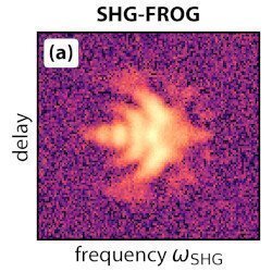
Graphic: IAP (University Jena)COPRA meets Python
Femtosecond laser pulses are among the shortest man-made events. To measure their temporal profile several techniques have been developed - most of which are known by their rather creative acronyms. Probably the most influential are frequency-resolved optical gating (FROG) and spectral phase interferometry for direct electric field reconstruction (SPIDER). In this work we developed a common pulse retrieval algorithm (COPRA) that can be applied to most of these measurements [1], independent of the specific experimental implementation. Besides its universality it has the advantage of being fast and robust against noise commonly encountered in experiments. We have published a Python package that implements pulse retrieval algorithms including COPRA for the measurement schemes mentioned above. It is available under an open-source license on github.
Published in Optica 6, 495-505 (2019)External link
Automated dual-tip SNOM for localized near-field investigations
Graphic: IAP (University Jena)Automated dual-tip SNOM for localized near-field investigations
Near-field optical microscopes with two independent tips for simultaneous excitation and detection can be essential tools for studying localized optical phenomena on the subwavelength scale, such as in plasmonic nanostructures, dielectric metasurfaces, or disordered photonic systems. In this work, we report on the implementation of a fully automated and robust dual-tip scanning near-field optical microscope (SNOM), in which the excitation tip is stationary, while the detection tip automatically scans the surrounding area. We have used this technique to map the near-field dipolar emission pattern of the surface plasmon-polariton on a gold film.
Published in Review of Scientific Instruments 90, 053705 (2019)External link
Submicrometer RGB filter arrays for a pixel size down to 0.5 μm
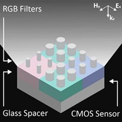
Illustration: IAP (University Jena)Dielectric resonators for imaging beyond conventional filters
Digital color imaging relies on spectral filters on top of a pixelated sensor, such as a CMOS image sensor. An important parameter of imaging devices is their resolution, which depends on the size of the pixels. For many applications, a high resolution is desirable, consequently requiring small spectral filters. Dielectric nanostructures, due to their resonant behavior and its tunability, offer the possibility to be assembled into flexible and miniature spectral filters, which could potentially replace conventional pigmented and dye-based color filters. We demonstrate submicrometer RGB filter arrays for a pixel size down to 0.5 μm.
Published in ACS Photonics 6, 1018-1025 (2019)External link
Chiral metasurfaces in a stack can yield chiral behavior .
Graphic: IAP (University Jena)Let's twist again: controlling the chirality of light
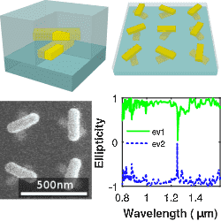
Both circularly and elliptically polarized light have a rotation direction in which its field vector is turning, giving light a handedness comparable to that of the DNA helix. This so called chirality of light can be tuned to different applications from sensing of chiral molecules to encoding in optical computers.
We experimentally demonstrated that, interestingly, a combination of non-chiral metasurfaces in a stack can yield chiral behavior while being easy to fabricate and understand. Moreover, our findings prove that chirality depends in part on Fabry-Perot-resonances from far-field interactions between the layers. This knowledge is very useful in future endeavors when chirality or other polarization properties have to be controlled from the design up.
Published in Opt. Express 27, 1236-1248 (2019)External link
Schematics of counterpropagating (CP) SPDC in a double-slot photonic crystal slab waveguide.
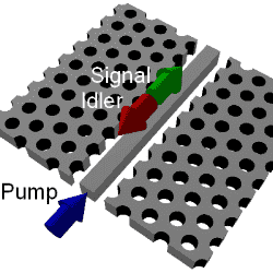
Graphic: IAP (University Jena)Factorizable counterpropagating photon pairs from periodic waveguides
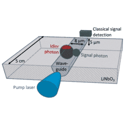
Spectrally unentangled photon pairs, aka factorizable pairs, are highly desired for implementation of heralded single-photon sources. In our work, we propose the use of photonic crystal waveguides (PCWs) for the realization of such sources. Using a design in lithium niobate, we numerically demonstrate that PCWs are capable of phase-matching a counterpropagating spontaneous parametric down-conversion process, which combined with PCWs' dispersion engineering property allows for reaching factorizability with a high degree of tunability. Such a source is uniquely suited for heralding applications, as the pair is separated directly at the source.
Published in Optics Letters 44, 69 (2019)External link
Light interaction with disordered materials.
Image: IAP (University Jena)Disorder-induced phase transitions in dielectric metasurfaces
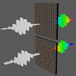
Metasurfaces made from dielectric nanoparticles typically possess a rather far-reaching inter-particle interaction, which is why their collective optical response is also quite sensitive to the particular arrangement of neighboring particles. We theoretically and experimentally studied the influence of disorder in the particle positions on the phase angle spectrum of light transmitted through such metasurfaces and found, for example, that the phase angle remains almost completely unaltered with increasing positional disorder, but only up to a certain critical threshold, at which the phase angle abruptly changes from normal to anomalous dispersion.
Published in Phys. Rev. Lett. 122, 015702 (2019)External link
Manipulation of magnetic dipole emission.
Graphic: IAP (University Jena)Manipulation of magnetic dipole emission
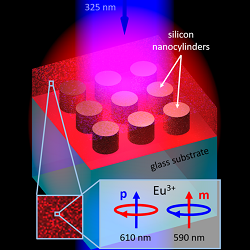
Mie-resonant dielectric metasurfaces are a viable platform for enhancing both electric and magnetic dipole transitions of fluorescent emitters. We study the enhancement of emission of Eu ions, featuring both electric and magnetic-dominated dipole transitions, by dielectric metasurfaces. We observe an enhancement of the Eu3+ emission associated with the electric (at 610 nm) and magnetic (at 590 nm) dipole transitions. The enhancement factor depends on the spectral proximity of the atomic transitions to the Mie resonances and the nature of the transition. Our results open new opportunities for bright nanoscale light sources based on magnetic transitions.
Published in Nano Lett. 19, 1015-1022 (2019)External link
Disorder Induced Pure Circular Dichrosim
Picture: IAP (University Jena)Directional and spectral shaping of light emission
We study how to manipulate the light emission with Mie-resonant silicon nanoantenna arrays on a glass substrate. When the spectral position of the silicon nanoantennas' magnetic dipole resonance overlaps with the intrinsic emission from the glass, the emission is selectively enhanced for certain spectral and spatial frequencies detemined by the design of the nanoantenna array. Furthermore, we observe that the nanoantenna array induces a reshaping of the emission pattern in the air half-space into a narrow lobe directed out of the substrate plane. This control of emission spectra and directionality is required for advances in multifunctional and "smart lighting".
Published in ACS Photonics 5, 1359-1364 (2018)External link
Waveguides for integrated SPDC spectroscopy.
Graphic: IAP (University Jena)Second-harmonic diffraction from a GaAs metasurface
Nonlinear photonic metasurfaces are an increasingly investigated field. In our group, we study the control of second-harmonic generation as the lowest order nonlinear frequency conversion in structured nonlinear materials. GaAs is a prominent candidate because it shows a strong second-order nonlinearity. But due to its crystal symmetry, no second-harmonic generation leaves the (100)-cut crystal surface when excited in normal incidence. The structured metasurface, however, is able to shape the second-harmonic radiation into the first diffraction orders of the periodic array.
Published in ACS Photonics 5, 1786-1793 (2018)External link
Atom-mediated pair generation using photonic bandgap modes
Graphic: IAP (University Jena)Disorder Induced Pure Circular Dichrosim
Many molecules in nature show different absorption properties for left and right handed circular polarized light. This so called circular dichroism is used to study the higher order structures of e.g. macromolecules. By introduction of rotational disorder to chiral wire pairs we were experimentally able to reproduce this effect and fabricate a metasurface with a pure circular dichroism several orders of magnitude stronger as in every natural molecule.
Published in ACS Photonics 5, 1773-1778 (2018)External link
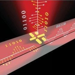
Scheme of a waveguide-integrated plasmonic nanoantenna for mode-selective polarization (de)multiplexing.
Image: IAP (University Jena)Atom-mediated pair generation using photonic bandgap modes
We propose the concept of atom-mediated pair generation, in which pair generation can take place only in the presence of a single 2-level emitter, relying on the bandgap evanescent modes of a nonlinear periodic waveguide. We show analytically, that the zero density-of-states of the bandgap modes prohibits pair generation in the nonlinear system, while adding an emitter to its vicinity mediates the process, in which a single photon is generated and its pair manifests itself as the emitter's excitation. This configuration can be the basis for new schemes in quantum spectroscopy and for the realization of hybrid sources of quantum light.
Published in Optics Letters 42, 4724 (2017)External link

