CZS Endowed Professor for Uwe D. Zeitner
New inspiration for the IAP and micro-optics
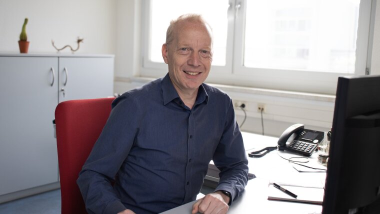

Published: | By: Ira Winkler
With pleasure! I am a physicist and studied in Jena from 1990 to 1995. I did my diploma at the Institute of Applied Physics (IAP) under Dr. Bernhard Kley and Prof. Kowarschik, then I did my doctorate as the first doctoral student of Prof. Frank Wyrowski here at the IAP on the topic of resonator-internal beam shaping with diffractive elements. I have been working at Fraunhofer IOF since 1999 - first as a scientist, later as a group leader and from 2017 as head of department. During this time, I have acquired and worked on many exciting projects relating to micro-optics, polarization measurement, optical design and laser lithography, as well as helping to develop technologies. For example, I was primarily responsible for the operation of the electron beam lithography facility (ELIT), which came to Fraunhofer IOF with the appointment of Andreas Tünnermann as Prof. Karthe's follow-up. In this context, the “Center for advanced Micro and Nano Optics” (CMN-Optics) was founded. Another milestone was the establishment of a second working group from the ZIK ultra optics in 2010, so that I was now responsible for around twenty employees. I also took on the administrative management of the Microstructure Technology research group at the IAP following the retirement of Bernhard Kley in 2017. Today, this group is successfully headed by Dr. Thomas Siefke.
After the restructuring of the IOF in 2020, I was appointed to the Scientific Directorate. After the coronavirus period, however, I felt the need for a change and successfully applied for the professorship for Technical Optics at Munich University of Applied Sciences (Hochschule München) in 2022.
I was in Munich for a total of two and a half years. Application driven works were the main focus there. I was already familiar with this from my time at the Fraunhofer IOF, but as a scientist I want to focus even more on the fundamentals. I also have my family here in Thuringia, so the CZS Endowed Professorship was very appealing to me. It is a professorship based on the Berlin model, which means that I can simultaneously take care of the training of young researchers at the University of Jena and conduct research at a non-university institution - in this case ideally at the partner institute IOF. In November 2024, I received the call and since May 9, I have been “CZS Endowed Professor for Micro- and Nanooptical Hybrid Systems - Design, Technology and Application”. The great thing is that the Carl Zeiss Foundation is funding the professorship with three million euros over the first five years.
I have made many new contacts from university and industry, including exciting start-ups. In Munich, I worked on a dynamic holographic writing process for microstructures - the project will continue there for another three years. This can be perfectly integrated into our projects on scaling nanostructuring down to square meter sizes.
However, the environment at Munich University of Applied Sciences cannot be compared with that in Jena: there, the focus is on industrial applications, even for students. Cooperation with industry is very close, but the university does not have its own large infrastructure for research.
As I was previously acting head of the Microstructure Technology research group and my professorship is thematically related to the subject area, some people are probably wondering whether I will be located there. This will be the case in terms of content, but with a separate group. Thomas Siefke's and my topics complement each other very well - we can develop many topics from the past together. However, we both set our own priorities. For me, the focus is particularly on lithography technology and the development of new materials for nano-optics, especially for ever shorter wavelengths. Thomas is concentrating on the further development of metrology in the nano range - in other words, the precise measurement of structures. I am developing new manufacturing processes for these structures. Together we want to raise nanostructuring for optical applications to a new level!
I would like to have a group of around 5 to 10 people, which I will build up gradually. It will remain one group - not another at the IOF. But of course I will also be working closely with the head of the Micro- and Nanostructured Optics Group, Dr. Falk Eilenberger - if only because of my role on the IOF Scientific Directorate.
I have my workplace at the IAP (room 212) and am always available - for new ideas or when things get stuck somewhere. I will also think about a name for my research group!
My lectures “Introduction to Optical Modeling” and “Micro & Nanotechnology”, which I gave as an adjunct professor here at the faculty were taken over by my colleagues Prof. Blahnik and Dr. Thomas Siefke. I envision a special lecture on physical optics to fill the thematic gap left by Prof. Wyrowski - this even closes a biographical circle.
Clearly the excellent facilities and the colleagues here! The launch of the new ELIT facility in the new research building at the end of 2025 is definitely a highlight in this context.
I'm also very grateful for the funding from the Carl Zeiss Foundation, as it offers a unique starting position for advancing new research topics.